Introduction:
This short briefing compares leading photovoltaic (PV) cell technologies and summarises where each stands in terms of record research-cell efficiency and representative commercial module performance (2024–2025). It focuses on high efficiency crystalline silicon architectures, perovskite based tandems and single junction perovskites, and established thin film CdTe and CIGS, highlighting key advantages, limitations, and commercial readiness.
1.1 Advanced single-junction crystalline silicon
Single‑junction crystalline‑silicon (c‑Si) cells use one p–n junction in a silicon wafer; modern records rely on n‑type wafers plus advanced surface passivation and low‑recombination contacts (TOPCon/HJT/back‑contact).
- The best research single-junction silicon cells have now surpassed 27% efficiency (records are ~27.8% certified, with 27.03% achieved on a 350 cm² commercial-sized device). [1,2]
- These records are achieved with n-type silicon and advanced passivated contacts (TOPCon, HJT, back-contact variants). [3,4]
Advantages:
Very mature, scalable supply chain; excellent field reliability and bankability; strong cost competitiveness.
Disadvantages:
Approaching the single‑junction efficiency ceiling; wafering/processing is energy‑ and capital‑intensive; front metallization (unless back‑contact) causes optical shading.
Key commercial variants:
a) TOPCon (Tunnel Oxide Passivated Contact)
TOPCon forms a passivated contact using an ultrathin tunnel SiO₂ plus doped poly‑Si, enabling carriers to pass while strongly suppressing recombination at the contact.
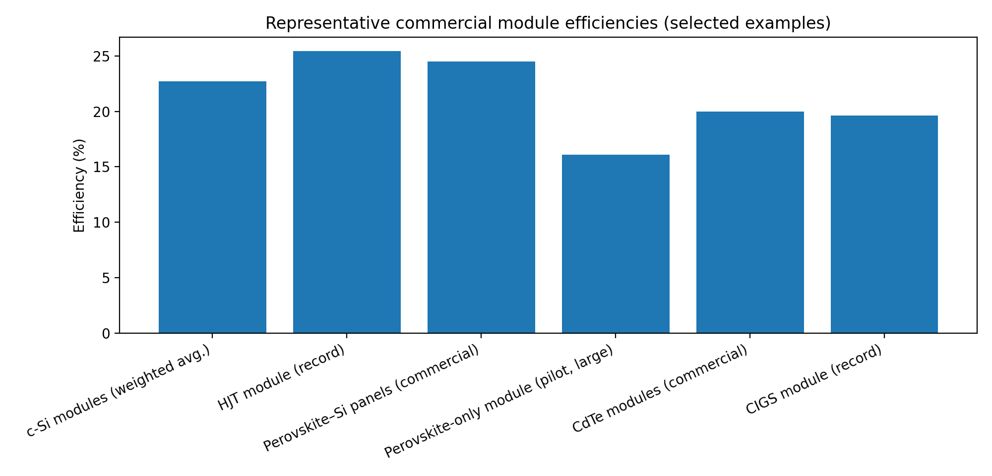
- Commercial modules: typically, ≈22–24% efficiency; a weighted average of 22.7% (Q4-2024 shipments) and best datasheet values of ≈24.8% were reported for c‑Si modules. [4]
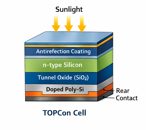
Advantages:
Boosts Voc and high efficiency uplift vs PERC with good yield; compatible with many existing Si production lines; strong bifacial performance.
Disadvantages:
Extra process steps (oxide + poly‑Si deposition/anneal) raise complexity; parasitic absorption in poly‑Si and tighter process windows can affect performance/cost.
b) HJT (Heterojunction)
HJT combines a crystalline‑Si wafer with thin amorphous‑Si:H passivation/junction layers and a transparent conductive oxide (TCO) for carrier collection, typically processed at low temperature.
- Trina has reported 25.44% for a large-area HJT module, certified by Fraunhofer CalLab. [5]
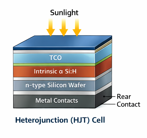
Advantages:
Very high open‑circuit voltage (Voc) and excellent temperature coefficient; naturally bifacial; strong low‑light performance.
Disadvantages:
Higher equipment cost (PECVD/sputtering) and tighter manufacturing control; relies more on TCO/Ag, and throughput can be lower than mainstream Si lines.
c) Integrated Back contact (IBC) / Hybrid Back Contact (HBC) / All Back Contact (ABC) back-contact cells
Back‑contact cells move both polarities of contacts to the rear, eliminating front shading. IBC uses interdigitated rear regions, so the front is contact-free (max light capture); HBC adds heterojunction‑style passivation with an IBC-like rear contact layout (usually more complex/costly to manufacture); ABC is a broad “all‑rear‑contact” umbrella term meaning all metallization and interconnections are on the back but the core idea is the same.
- Put contacts on the rear to remove front shading; record silicon cells around 27–28% are based on such high-end architectures. [1,3]
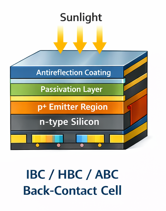
Advantages:
Maximum light capture (no front grid shading) and premium aesthetics; among the highest single‑junction Si efficiencies; strong performance when area is limited.
Disadvantages:
Rear patterning/alignment is complex and can raise cost; more demanding interconnection and series‑resistance control; manufacturing yield can be harder to maintain.
1.2 Perovskite–silicon tandem cells
Perovskite–Si tandems stack a wide‑bandgap perovskite top cell over a silicon bottom cell so high‑ and low‑energy photons are harvested more efficiently than in a single junction (2‑terminal monolithic or 4‑terminal).
- Crystalline-silicon / perovskite tandems are now the highest among emerging low-temperature thin-film + silicon hybrid tandems.
- LONGi reports 34.85%(in April) certified cell efficiency for two-terminal perovskite–Si tandems, however it has increased to 35% by November (certified by NREL). [6]
- Fraunhofer ISE + Oxford PV have demonstrated 25% efficient full-size tandem modules with glass–glass encapsulation. [6]
- Oxford PV later announced residential-sized perovskite–silicon modules with 26.9% efficiency and has reported first commercial panels at 24.5% module efficiency. [8,9]
- These results put tandem cells above the Shockley–Queisser detailed-balance limit for single-junction cells (≈33% at 1 sun) and above silicon’s own single-junction limit (≈32%). [13]
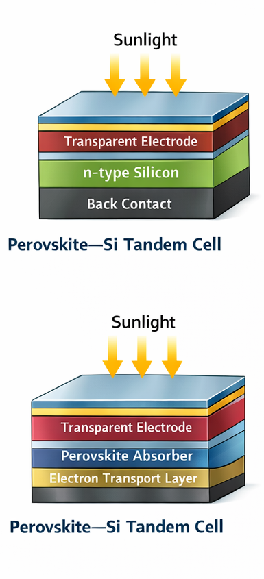
Advantages:
Highest demonstrated efficiencies and best path to >30% modules; more power from the same area (higher W/m²); potential premium option where space is constrained.
Disadvantages:
Long‑term stability and encapsulation are still key hurdles; scale‑up/yield control for large‑area perovskite layers is challenging; lead management and recycling requirements must be addressed.
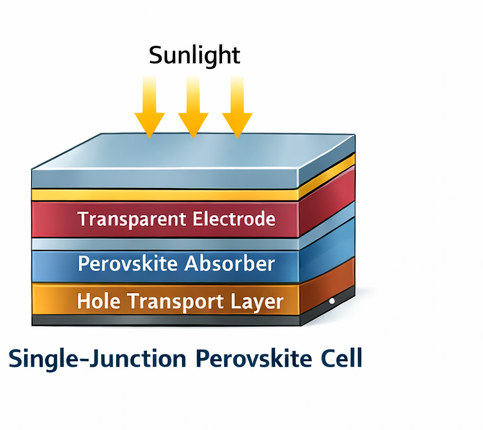
1.3 Single-junction perovskite cells:
A single-junction perovskite solar cell uses one perovskite absorber layer (typically ABX₃ halide perovskite) sandwiched between selective charge-transport layers and electrodes. The most common stacks are n–i–p (TCO / ETL / perovskite / HTL / metal) and p–i–n (TCO / HTL / perovskite / ETL / metal), with the perovskite acting as the main light absorber and junction-forming layer.
- State-of-the-art single-junction perovskite cells now reach ≈26.3% certified efficiency in the lab. [1]
- Efficiency reviews summarise single-junction perovskite records above 26% and perovskite–silicon tandems above 30%. [3]
- Perovskites are therefore competitive with crystalline silicon in efficiency, but stability, degradation, and end-of-life lead management remain key commercial challenges. [14]
Advantages:
Very high efficiency potential with thin, low‑temperature processed layers; bandgap tunable by composition; can be made lightweight/flexible with suitable substrates.
Disadvantages:
Moisture/heat/UV sensitivity and ion migration can cause degradation; hysteresis/defect control remains important; lead‑containing chemistries require containment and end‑of‑life handling.
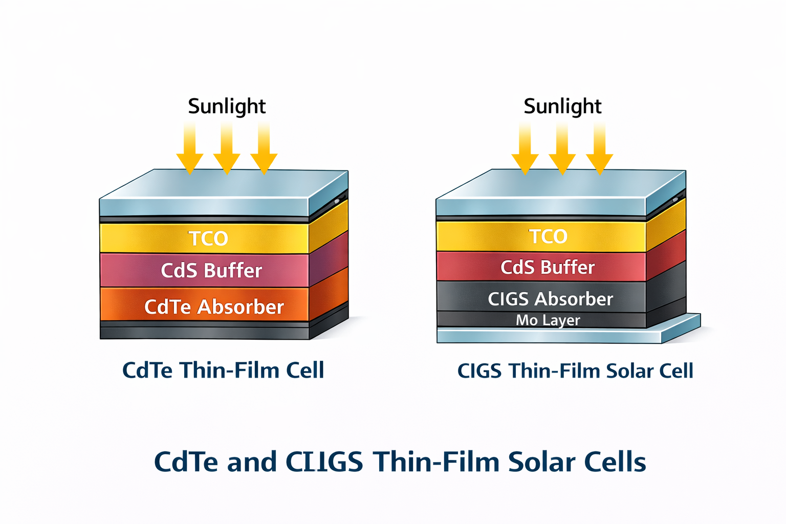
1.4 Thin-film CdTe and CIGS
Thin‑film technologies use micrometre‑scale absorbers on glass or flexible substrates. CdTe uses a CdTe absorber with CdS buffer and a TCO front contact; CIGS uses a Cu(In,Ga)Se₂ absorber with buffer + TCO. These are not as “headline grabbing” as perovskites now, but they remain important for utility-scale (CdTe) and flexible (CIGS) niches.
From the NREL chart: [1]
- CdTe research cells are at ~23.1% (record); commercial CdTe modules are approaching ~20% efficiency. [1,4]
- CIGS research cells are at ~23.6% (record). Commercial modules span ~17–20%, with a reported record of 19.64% for a 30×30 cm CIGS module. [1,12]
Advantages:
Strong light absorption enables thin layers; generally good temperature and low‑light performance; CdTe is bankable at utility scale, while CIGS enables flexible/lightweight products.
Disadvantages:
CdTe depends on tellurium supply and requires careful cadmium stewardship; CIGS uses In/Ga (cost/supply) and can be harder to scale uniformly to very large areas (often also uses CdS buffers).
Comparison table of main PV cell technologies
| Cell technology | Typical structure / contact concept | Best research cell η (approx.) | Typical commercial module η (2024–25) | Key strengths / notes |
|---|---|---|---|---|
| Advanced c-Si (PERC → TOPCon, HJT, IBC) | n-type wafers; passivated contacts (TOPCon, HJT), sometimes back-contact layouts | ≈27.8% record; 27.03% for 350 cm² device [1,2] | c-Si modules: weighted-average 22.7% (Q4-2024 shipments); max ~24.8% [4] | Mature, scalable, rapidly improving; cost competitive. |
| TOPCon (as a subset of above) | Ultra-thin SiO₂ tunnel oxide + doped poly-Si passivated contacts | Included in silicon record above [1–3] | Typically, within above c-Si range (≈22–24%); TOPCon replacing PERC [4] | Becoming the new “workhorse” high-efficiency cell for mass production. |
| HJT (heterojunction) | c-Si wafer + a-Si:H layers + TCO on both sides (often bifacial) | Around 27% lab-scale HJT cells [2] | Record HJT module 25.44% (certified) [5]; best commercial products ~24.8% [4] | Very high Voc, good high-temperature behaviour; currently higher cost. |
| Silicon back-contact (IBC / HBC / ABC) | All or most contacts on rear (no front shading), often combined with passivated contacts | Contribute to ≈27% Si records [2,3] | Premium products within the highest c-Si range (~24–24.8%) [4] | Highest-end crystalline products; ideal where roof area is limited. |
| Perovskite–Si tandem | Wide-bandgap perovskite top cell + Si bottom cell, monolithic 2T | 34.85% certified 2T tandem cell [6] | Full-size tandem modules at 25% [7]; record module 26.9% [8]; commercial panels 24.5% [9] | Clear efficiency champion; future mass-market premium technology. |
| Single-junction perovskite | Thin perovskite absorber with transport layers on TCO substrate | ≈26.3% certified record [1] | Certified minimodule 24.0% [10]; large-area pilot modules ~16.1% [11] | Huge potential, but stability and lead are still under active development. |
| CdTe thin-film | CdTe absorber on glass with CdS buffer, TCO front contact | ≈23.1% record research cell [1] | ≈20% commercial modules [4] | Strong in large-scale plants; excellent temperature behaviour. |
| CIGS thin-film | CIGS absorber on glass or flexible foil, with buffer and TCO | ≈23.6% record research cell [1] | ~17–20%; reported record module 19.64% (30×30 cm) [12] | Good for flexible/lightweight modules; higher cost per W in many markets. |
Figures
Figure 1. Best research efficiencies (selected PV technologies).
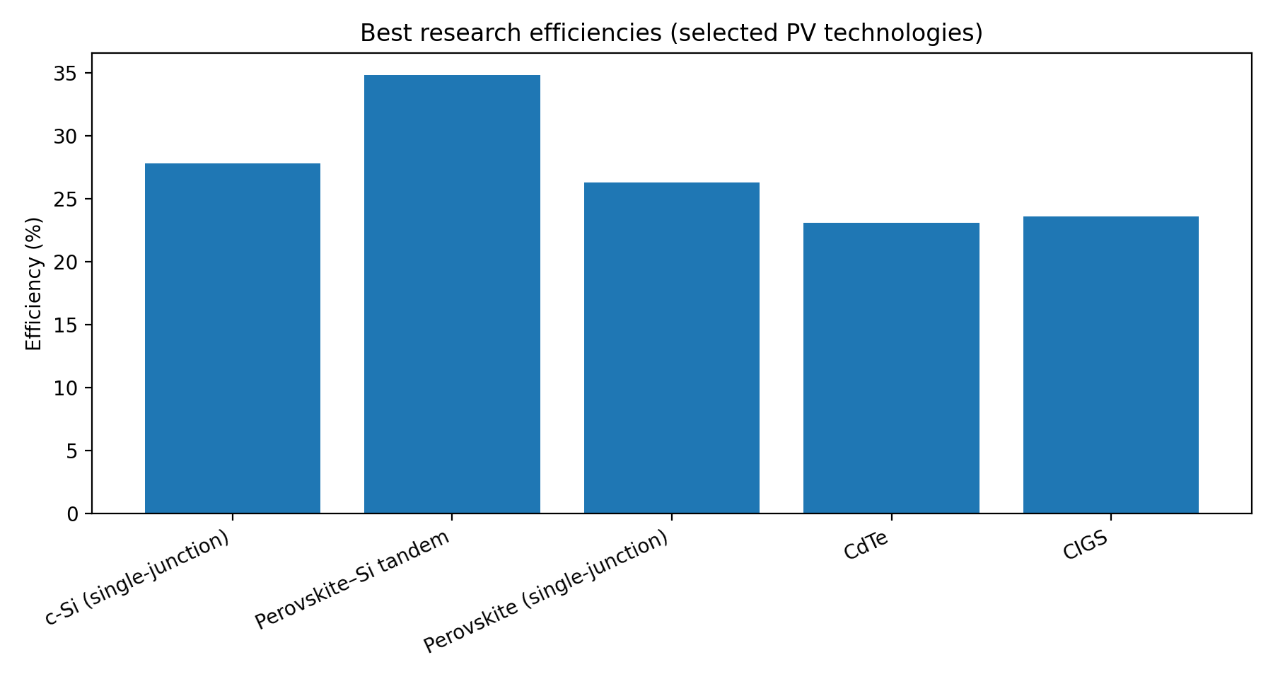
Figure 2. Representative commercial module efficiencies (selected examples).
Conclusion:
Modern PV technology is converging on high-efficiency n-type crystalline-silicon platforms (especially TOPCon and HJT) as the mass-market workhorses, while back-contact designs provide premium efficiency where area is limited. Perovskite-silicon tandems have demonstrated the highest certified cell efficiencies and remain the clearest route to >30% module efficiency, but long-term stability, large-area yield, encapsulation, and lead management must be addressed for broad deployment. Single-junction perovskites offer lightweight, low-temperature processing and fast efficiency progress, yet durability and end-of-life handling are still key constraints. Established thin-film CdTe and CIGS continue to play important roles: CdTe is strongly positioned for bankable utility-scale plants, while CIGS enables flexible and lightweight products, though materials supply and large-area uniformity remain important considerations. Overall, incremental gains will come from continued optimization of silicon and manufacturing, while tandems and stable perovskites represent the main path to step-change efficiency and new application spaces.
References
[1] National Renewable Energy Laboratory (NREL). Best Research-Cell Efficiency Chart (rev. 11 Dec 2025). [2] Tong, H. et al. “Total-area world-record efficiency of 27.03% for 350.0 cm² commercial-sized single-junction silicon solar cells.” Nature Communications (2025). [3] Green, M.A. et al. “Solar Cell Efficiency Tables (Version 66).” Progress in Photovoltaics: Research and Applications (2025). [4] Fraunhofer ISE. Photovoltaics Report (updated 31 Oct 2025). [5] Reuters. “Trina Solar sets world record for solar technology” (6 Jan 2025) – reports 25.44% HJT module efficiency certified by Fraunhofer CalLab. [6] LONGi. Press release: LONGi achieves 34.85% efficiency for perovskite-silicon tandem solar cell (15 Apr 2025), certified by NREL. [7] Fraunhofer ISE press release: Oxford PV and Fraunhofer ISE develop full-sized tandem PV module with record efficiency of 25% (31 Jan 2024). [8] Oxford PV press release: Oxford PV debuts residential solar module with record-setting 26.9% efficiency (19 Jun 2024). [9] Oxford PV press release: “20% more powerful tandem solar panels enter commercial distribution” (30 Sept 2025) – reports 24.5% module efficiency for first panels on the market. [10] NREL news release: Collaboration between NREL and CubicPV pushes perovskite minimodule performance to 24.0% certified efficiency (2025). [11] pv magazine. “Chinese PV industry brief: UtmoLight begins perovskite solar module production at GW-scale facility” (7 Feb 2025) – reports 16.1% efficiency on a 2.8 m² perovskite module in pilot production. [12] pv magazine. “Avancis claims 19.64% efficiency for CIGS module” (4 Mar 2021). [13] Shockley, W.; Queisser, H.J. “Detailed Balance Limit of Efficiency of p-n Junction Solar Cells.” Journal of Applied Physics 32, 510–519 (1961). [14] Liu, K. et al. “Lead (Pb) management in the entire life cycle of highly efficient perovskite solar cells.” Energy & Environmental Science (2024).
-
Enectiva supports performance monitoring and KPI-based analysis of PV plants through Modbus-enabled data acquisition and integration with industry-standard monitoring and control systems.
-
Read more about solar-panel applications and efficiency comparisons in Solar panel technology Solar Panel Technology
For more information or to get started, contact us directly at sales@enectiva.com or +420 222 766 950.